
In a groundbreaking development that promises to reshape the landscape of digital displays and advanced sensing, Swiss researchers at ETH Zurich have engineered organic light-emitting diodes (OLEDs) so small they are 100 times tinier than a human cell. This monumental miniaturization, spearheaded by Professor Chih-Jen Shih, paves the way for a new era of ultra-sharp screens, high-precision microscopes, and advanced light control mechanisms crucial for the future of robotics and smart manufacturing.
The Dawn of Nanoscopic Illumination
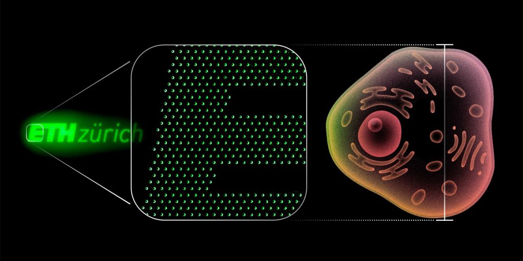
Traditional OLED technology is already a staple in premium smartphones and televisions, celebrated for its vibrant colors and deep blacks. However, the team at ETH Zurich has pushed the boundaries of what’s possible, developing a novel one-step fabrication process that shrinks these diodes to an unprecedented scale. With individual pixels measuring approximately 100 nanometers – an astonishing 50 times smaller than current state-of-the-art OLEDs – this innovation boasts a pixel density 2500 times greater than before.
To put this into perspective, the researchers demonstrated their achievement by forming the university’s logo from 2,800 individual diodes within a structure only 20 micrometers tall – roughly the size of a single human cell. This corresponds to a theoretical resolution of an incredible 50,000 pixels per inch (ppi), making ultra-sharp screens for future wearables and near-eye devices a tangible reality.
Reshaping Robotics and Smart Manufacturing Perception
The implications of such miniature light sources extend far beyond consumer electronics, offering transformative potential for industrial and robotic applications:
- Advanced Machine Vision & Perception: For robotics, the ability to generate incredibly detailed images means a quantum leap in visual perception. Robots could achieve unprecedented precision in inspection, quality control, and micro-manipulation tasks. Imagine autonomous systems with vision capabilities that rival or even surpass human sight at microscopic levels, enabling intricate assembly or defect detection previously impossible.
- High-Resolution Human-Machine Interfaces (HMIs): Ultra-sharp, miniature displays could revolutionize how human operators interact with complex robotic systems. Near-eye displays for augmented reality applications in industrial settings, providing real-time data overlays or guiding intricate repairs, would benefit immensely from this pixel density.
- Sensitive Sensors & Measurement: Beyond displays, these nano-OLEDs can function as powerful light sources for highly sensitive biosensors. Capable of illuminating the most minute areas of a sample, they could enable the detection of signals from single cells, offering profound advancements for medical robotics, lab automation, and bio-manufacturing processes.
- On-Chip Optical Data Transmission: The technology could power new optical systems that transmit data by shaping light directly on a chip. This means faster, more energy-efficient data communication within industrial IoT (IIoT) and edge computing devices, crucial for real-time analytics and distributed intelligence in smart factories.
- Mini Lasers and Precision Tools: When bundled, these nano-OLEDs can construct powerful mini lasers, offering new possibilities for precision cutting, welding, or material processing at the micro-scale within automated production lines.
Phased-Array Optics: Controlling Light Without Moving Parts
One of the most exciting aspects of this breakthrough is the ability of these diodes, being smaller than the wavelength of visible light, to control emitted light with exceptional precision. When arranged closely, light waves from neighboring pixels can interact, reinforcing or canceling each other. This phenomenon is the basis of phased-array optics, allowing for electronic steering and focusing of light beams without any moving parts.
This capability promises holographic displays and advanced optical systems that can dynamically shape light for various applications, including potentially creating new types of 3D imagery around viewers through meta-pixels. Such control over light at the nano-scale opens doors for innovative sensory input for robots, dynamic projection mapping in industrial spaces, or advanced security and identification systems.
The Future is Bright (and Tiny)
The manufacturing process itself is highly compatible with standard lithography processes used in computer chip production, thanks to the use of silicon-nitride membranes that are 3,000 times thinner than conventional metal masks. This ease of integration suggests a faster path from lab to industrial application.
Published in Nature Photonics, this research by ETH Zurich marks a pivotal moment in display and photonic technology. For the robotics and smart manufacturing sectors, it heralds an era of unprecedented visual acuity, sensing precision, and compact, intelligent optical systems, pushing the boundaries of what automated systems can perceive and achieve.
Connect with the CTO ROBOTICS Media Community
Follow us and join our community channels for the latest insights in AI, Robotics, Smart Manufacturing and Smart Tech.


CTO Robotics
CTO Robotics is a global media and consulting company dedicated to robotics, automation, artificial intelligence, and emerging technologies. We create high-impact content that reaches engineers, decision-makers, and innovators worldwide. Through articles, videos, social media campaigns, and community-driven storytelling, we help companies showcase their technologies, strengthen their brand, and connect with the right audience. Much like Interesting Engineering or Wevolver, our mission is to bridge the gap between technology providers and industry professionals — turning innovation into visibility, and visibility into growth. 👉 Whether you are launching a new product, building your brand, or looking for global recognition, CTO Robotics is your media partner for exposure, credibility, and business opportunities.
All stories by: CTO Robotics


0 Comments